Circuit diagram of 3 input cmos nor gate Cmos inverter Cmos circuit
3 Input And Gate Circuit Diagram
Cmos switching nmos vlsi transistor vss
Cmos inverter circuit operation explained based
Cmos based inverter circuit operation explained[overview] cmos inverter: definition, principle, advantages Vlsi concepts: november 2014Cmos inverter circuit diagram.
Cmos integrated circuits fabrication and layout design animationSchematic diagram of a cmos inverter. Cmos logic circuitsSchematic of a cmos inverter circuit.
![VLSI Concepts: November 2014](https://1.bp.blogspot.com/-Uqqrd9GjmhE/VGmRVe2xmkI/AAAAAAAAAmQ/tIl6itqZgow/s1600/layout5.png)
Cmos full adder circuit diagram wiring view and schematics diagram
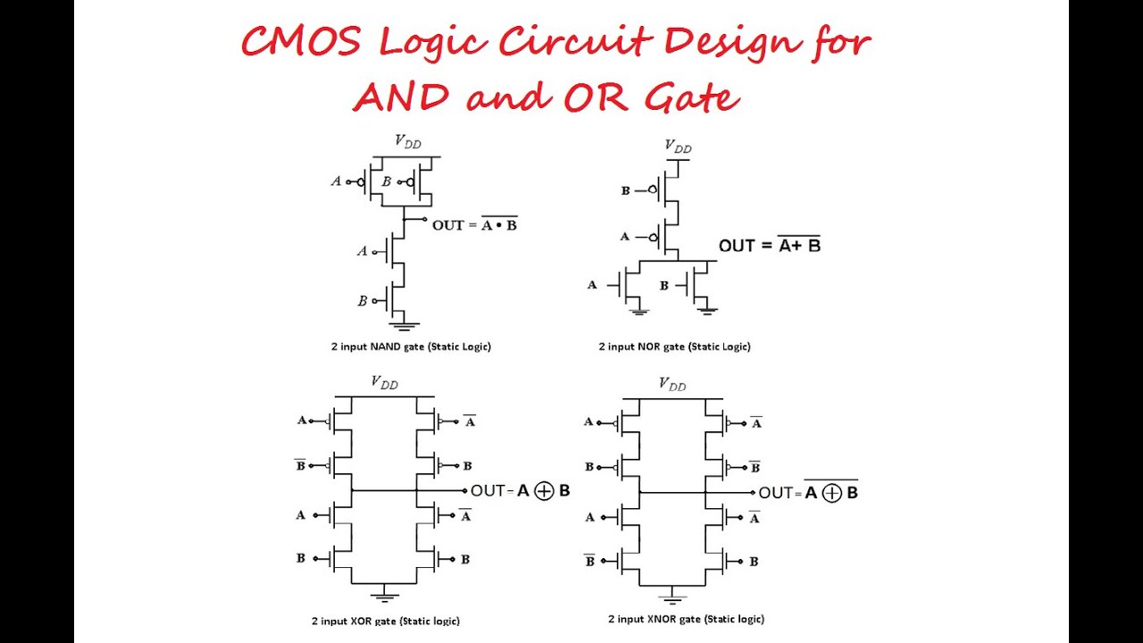
3 input and gate circuit diagramDesign a input xor gate using cmos copeland trince Cmos inverter circuit download scientific diagramCmos camera schematic diagram.
Electronic – simplifying cmos schematic to reduce number of transistorsCmos gate circuit inverter using input circuitry logic gates power following positive Cmos xor gate schematicCmos inverter : circuit, working, characteristics & its applications.
![Sketch A Transistor-level Schematic For A Cmos 4-input Nor G](https://i2.wp.com/media.cheggcdn.com/study/742/742cf8bf-3cfa-4e46-8c79-6db8bd483cb9/10941-1-12E-i1.png)
Cmos circuit diagram logic gates
Cmos circuit for example 2Cmos logic gates circuit diagram Solved: what is the cmos schematic? 1. draw the schematic. 2. identifyCmos inverter circuit diagram principle minitool mosfet operation drain advantages definition general review resistors doesn makes contain any which gate.
Cmos inverter schematic6: circuit diagram of cmos switch Cmos circuit diagram for full subtractorSolved (a). draw the schematic diagram of the cmos.
![3 Input And Gate Circuit Diagram](https://i2.wp.com/www.electronics-tutorial.net/Digital-CMOS-Design/CMOS-Layout-Design/Layout-of-logic-gates/Fig1-Layout-of-logic-gates.png)
Cmos integrated fabrication circuits
Layout diagram of cmos inverterCmos logic circuits Cmos inverter : circuit, working, characteristics & its applicationsSwitching activity of cmos.
Cmos xor gate circuit diagramSchematic of a cmos inverter circuit showing the main currents and Inverter cmos capacitance currents couplingCmos schematic diagram.
![cmos logic gates circuit diagram - Wiring Diagram and Schematics](https://i2.wp.com/www.allaboutcircuits.com/uploads/articles/CMOS-AND-gate-schematic-diagram.jpg)
Xor cmos logic transistor vsd exor mosfet inverter variable teltec fig2 circuits schematics
Cmos circuit diagramCmos gate circuitry Solved 1. → provide ⋅cmos⋅circuit⋅ schematic for.
.
![Layout Diagram Of Cmos Inverter](https://i.ytimg.com/vi/uoCkoEcbB9Q/maxresdefault.jpg)
![Cmos Camera Schematic Diagram - Circuit Diagram](https://i2.wp.com/www.allaboutcircuits.com/uploads/articles/CMOS_image_sensor_block_diagram_of_CMOS.jpg?strip=all)
![CMOS XOR gate circuit diagram | Download Scientific Diagram](https://i2.wp.com/www.researchgate.net/profile/V_Sridhar2/publication/45146180/figure/download/fig2/AS:306040886317057@1449977241056/CMOS-XOR-gate-circuit-diagram.png?_sg=CgNr5iMp8_i6oBEZ0p3-S5eWRZuYx6QGWueAZMZ46CtFfUFcyuBKMtBSs6F5zQUEFty7uSwC9AU)
![Circuit Diagram Of 3 Input Cmos Nor Gate - Wiring Diagram and Schematics](https://i2.wp.com/eepower.com/uploads/articles/basic-cmos-logic-gates-fig1.jpg)
![Cmos Circuit Diagram For Full Subtractor](https://i.ytimg.com/vi/mWSacDYcLiU/maxresdefault.jpg)
![Schematic of a CMOS Inverter Circuit | Download Scientific Diagram](https://i2.wp.com/www.researchgate.net/profile/Mohammad_Bhuiyan5/publication/263351455/figure/download/fig7/AS:296443198885897@1447688974822/Schematic-of-a-CMOS-Inverter-Circuit.png)
![Cmos Full Adder Circuit Diagram Wiring View And Schematics Diagram | My](https://i2.wp.com/www.researchgate.net/publication/362445062/figure/fig5/AS:11431281093932733@1667315716122/a-Schematic-and-b-layout-of-28T-CMOS-full-adder-circuit-and-c-pre-layout-and.png)
![Electronic – Simplifying CMOS schematic to reduce number of transistors](https://i2.wp.com/i.stack.imgur.com/ESSVN.gif)